This product was designed by LeoNerd's Store.
By buying this product you support original hardware creators.


Develop applications using the AVR 2-series ATtiny824
Summary
- ATtiny824 breakout
- UPDI+ programming header
- Status LED
- Reset button
What is it?
This board holds an AVR ATtiny824 microcontroller, providing access to all of the IO pins. It adds power supply decoupling capacitors, an LED, a button, and UPDI programming header to make a convenient self-contained development board for small microcontroller projects.
The LED is attached to the PA7 pin via a 2k2 current-limiting resistor.
The button is attached to the PA0 UPDI/RESET# pin via a series resistor to prevent damage in case of drive contention. Note that the PA0 pin defaults to UPDI mode. Switching the pin to RESET mode will require the use of a 12V-capable UPDI programmer if you want to program the chip after this.
The board also provides a programming header in the AVR standard 2x3 layout. Note that this will requires a UPDI-capable programmer. An SPI-style ISP programmer will not work with this chip. This programming header also includes the USART.0 TX and RX signals in "UPDI+" layout, allowing single-cable programming and debug with a suitable programmer.
Finally, an extra 2-pin header is provided with another VCC and GND pin in case additional connections are required.
Reference icons are placed next to the pins used by the USART, I²C and SPI modules, and where the LED is connected, to remind you what functions those pins usually perform.
This board is supplied with two 7 pin header strips for the IO pins and one 2x3 pin for the programming connector.
ATtiny824
The ATtiny824 is one of the new AVR 2-series microcontrollers, containing xmega-style peripherals. These are more powerful and flexible than previous generations of ATmega and ATtiny chips.
This particular chip contains 8 KiB of flash and 1 KiB of RAM on an AVR CPU clocked at 20 MHz. It provides three 16bit PWM-capable timers, a 16bit realtime counter, two USARTs with fractional baud rate generator, a master/slave capable SPI interface, I²C interface, analog comparator, 12bit differential ADC with PGA, and in total 12 IO pins split across two ports. It also provides a 6-channel event system and configurable custom logic block that can route events between peripherals without waking the CPU.
Compared to the ATtiny814, this chip has twice the SRAM, adds a second TCB unit, a second USART unit, and fixes some bugs and missing features with the design of the TCB. It does remove the 12-bit dual output TCD timer and DAC output, though.
More information can be found on Microchip's website at https://www.microchip.com/wwwproducts/en/ATTINY824
Why did you make it?
I wanted to experiment with the new AVR 2-series chips, but couldn't find any maker-oriented hardware for them.
What makes it special?
I believe this may be the first use of an ATtiny824, outside of the development boards produced by Microchip themselves.
Related Products
| Size | AVR 1-series | AVR 2-series |
|---|---|---|
| 8pin, 4KiB flash | ATtiny412 | - |
| 14pin, 8KiB flash | ATtiny814 | ATtiny824 |
| 20pin, 16KiB flash | ATtiny1616 | ATtiny1626 |
| 24pin, 32KiB flash | ATtiny3217 | ATtiny3227 |
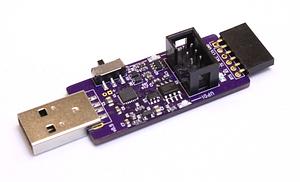
AVR UPDI Programmer with 12V A USB UPDI programmer with a second serial port and 12V pulse generator
AVR UPDI Programming Cable
 Flash firmware onto an AVR microcontroller chip via UPDI
Links to code and documentation
No additional links provided for this product.
Product HS Code: 853710
Shipping policy
No information available.
Here are some extras that might be useful for your project!
ATtiny824 Development Board
Sold by LeoNerd's Store
$14.98
No tax for United States [change]
Stock available: 3
The seller

Custom test equipment, digital electronics, microcontrollers, C and Perl programming alongside them.